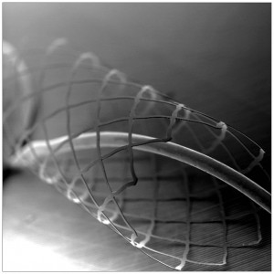
Sputtered films can be fabricated with high feature resolution, as small as 5 microns in lateral dimension for a device of 25 microns in thickness. For the same device the thickness varies by only ±250 nm. Devices can be fabricated with great scalability and repeatability, since the manufacturing is based on micro system technology processes. Devices for minimal-invasive procedures can be miniaturized and fabricated accurately, allowing for smaller catheter diameters. Industrial devices can be made small and lightweight, reducing dimensions and weights of components, while having optimized force-stroke relationships.
Back to benefits.

