ACQUANDAS‘ fabrication method involves a series of microsystem technology processes, which allows ACQUANDAS to produce components of high resolution, with excellent mechanical properties and unmatched freedom of design. The main processes are UV-lithography, magnetron sputtering and wet chemical etching.
UV-Lithography
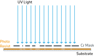
UV-Lithography is a common structuring technique in microsystems technology. A photosensitive resist is exposed to UV-light via a glass mask that is partly covered with chromium. Special developers are used to dissolve exposed areas of the resist while unexposed areas remain intact. After cleaning, a resist pattern remains on the substrate. The resolution of standard UV-lithography using Hg lamps is in the sub-micron range.
Magnetron sputtering
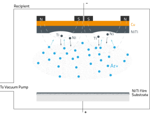
Magnetron sputtering is an ultra-high vacuum deposition technique. Many materials can be sputter deposited, among them materials we currently focus on, namely Nitinol, Mg and Fe alloys. Inside an evacuated deposition chamber, Ar ions are accelerated towards a target, a disc or rectangular shaped part, consisting of the alloy that is about to be deposited. Due to ion bombardment, atoms are released from the target and deposited on the substrate opposite.
ACQUANDAS has great expertise in depositing functional materials such as Nitinol, spanning from precise target material specifications to engineering aspects and deposition parameters.
Wet Chemical Etching
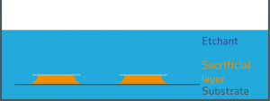
Wet chemical etching is a technique where specific etchants are employed to selectively remove material. We use wet chemical etching to remove certain parts of a seed layer or to completely remove sacrifical layers in order to obtain freestanding structures.
ACQUANDAS combines more than 30 years of experience in the production of the above-mentioned intelligent materials by using thin film fabrication methods. Learn more about our fabrication method from our literature section.


